Hardware Development Demonstration - STM32 Powered Alarm Clock
The purpose of this project was to demonstrate hardware development capabilities using an STMicroelectronics STM32 ARM powered microcontroller.
PCB Layout (3D render) screen capture

The Alarm Clock gadget takes user inputs of time and alarming-time and outputs these values through an LCD character display and buzzer.
Currently implemented software functions include:
- Display interfacing through through 6-button user interface
- Set current time (hardware RTC; currently 24-hour display format)
- Set alarm time
- Alarm when current time and alarm time equal
- Snooze alarm (5-minute intervals)
- Disable alarm (auto-recurring next-day)
Power is supplied to the device through a surface-mounted micro-USB connector (5 Vdc, SELV). 3.3 Vdc is supplied to the microcontroller from the fixed-output of a 5-3.3v LDO regulator.
Six through-hole momentary push button switches provide a conventional interface with OK/Enter, Back, Up, Down, Left, and Right mappings. Some of the buttons serve multiple functions, e.g. Back acts to return from menus and to disable the alarm once active.
The microcontroller and buttons are interfaced via an asynchronous parallel-in, serial-out shift register. While the STM32 microcontroller offers more than enough GPIO to handle the buttons and display, the use of the shift register IC was a separate learning opportunity.
An 8-bit (parallel), 20x2 LCD character display assembly (with on-board display controller) is used as the primary user display. This display is driven in parallel directly from the microcontroller.
The 5V buzzer is driven by an NPN transistor which is switched by a bit-banged square wave from the uC's GPIO.
The microcontroller is programmed via serial-wire debug through an ST-Link V3 programmer.
The internal high-speed clock is utilized, and a low-speed external 32.768 quartz-crystal oscillator circuit is used for the RTC time keeping.
A USB ESD protection diode array IC is used to prevent damage to the microcontroller during handling.
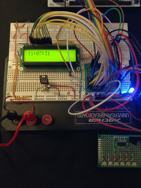
The shift register and STM32 microcontroller were each installed onto their own breakout boards. A 5V-3.3V regulator was connected to the breadboard's power rail. Decoupling capacitors were installed directly on the power rail. Jumpers were connected as necessary - and thus the Alarm Clock came alive:
Schematic capture using EasyEDA:

Since the Schematic Capture was conducted in EasyEDA, the trace layout was also formed in EasyEDA. Generally, the order of operations was to place:
- Microcontroller dead center,
- Edge-mounted headers and USB,
- Push button switches mounted in standard-layout on reverse-side,
- Power components placed near power input connector,
- Decoupling capacitors placed near Vdd/Vss pins of MCU,
- Shift register placed,
- All other hardware - routes connected.
PCB Layout screen capture

The Gerber files, BOM, and pick-and-place files were generated through EasyEDA, uploaded to JLCPCB, and any part orientations were corrected in JLCPCB's online board viewer.
Two assembled boards, and three bare boards were received from the manufacturer in short order. They looked and functioned great!

The first batch of PCBs had a few minor mistakes:
- MCU BOOT0 pin was routed in series with NRST pin, but the MCU requires a certain order of operations to program to internal Flash memory. I had to cut the NRST trace and route a jumper wire to the SWD header (leaving the BOOT0 pin floating). Luckily, this has allowed for suitable firmware flashing.
- Size of mounting holes: The mounting holes are too small - this should be fine for a prototype. In the future, I'll enlarge them.
- Reliance on bit-banging the buzzer. In the future, it would be nice to rely on the hardware clock, or an external oscillator, to drive the buzzer instead of GPIO toggling.
- Missing decoupling capacitor on one power port of the MCU. So far this has not seemed to create an issue. I manually added the capacitor during the internal flash/BOOT0 pin debug, but results were identical.
- LCD contrast resistances: From breadboard to prototype, I miscalculated the voltage divider for the display contrast. For this prototype, I simply trimed the resistance as needed.
- Generally, I could have used much smaller SMD parts to avoid crowding, especially in the LSE RTC circuit.
See src/main.c for all relevant code with embedded comments
Programming Language: C Flash size: 13.55 KB / 64 KB available (21% used / 79% avail.)
