GithubHelp home page GithubHelp logo

nullobject / sdram-fpga Goto Github PK

View Code? Open in Web Editor NEW
109.0 15.0 28.0 122 KB

A FPGA core for a simple SDRAM controller.

Home Page: https://www.joshbassett.info/sdram-controller/

License: MIT License

VHDL 100.00%
fpga sdram memory controller

sdram-fpga's Introduction

SDRAM Controller

Because synchronous dynamic RAM (SDRAM) has complex timing and signalling requirements, a memory controller is necessary to avoid having to deal with the nitty-gritty details when reading or writing to memory. Its job is to hide the complexity of things like row and column addressing, precharging, and refreshing. Instead it lets us treat SDRAM just like plain old static memory.

This SDRAM controller provides a symmetric 32-bit synchronous read/write interface for a 16Mx16-bit SDRAM chip (e.g. AS4C16M16SA-6TCN, IS42S16400F, etc.).

Even though the SDRAM chip only has a 16-bit data bus, the controller uses a 32-bit data bus because it is more efficient to burst multiple words from the SDRAM than it is to do individual reads and writes.

Documentation

Signals 🚥

name direction description
reset input resets the SDRAM controller when asserted
clk input clock
addr input address bus
data input input data bus
we input write enable
req input requests a read or write operation when asserted
ack output asserted when a request is accepted by the SDRAM controller
valid output asserted when there is valid data on the output data bus
q output output data bus

Reset

The reset signal can be used to reset the internal state machine for the SDRAM controller.

Clock

The clk signal is the system clock used by the SDRAM controller.

Ideally, it should be different to the SDRAM clock (i.e. the clock for the actual SDRAM chip). By adjusting the phase relationship so that the SDRAM clock leads the system clock, we can ensure that the SDRAM output signals arrive in time to meet our timing constraints.

Address Bus

The addr signal should be set to the address of the memory location being accessed.

Input Data Bus

The data signal should be set to the 32-bit value to be written to the memory location at the given address.

Write Enable

The we signal should be asserted when you want to write to the SDRAM. It should be asserted together with the req signal.

Request

The req signal should be asserted when you want to read or write to the SDRAM. When making a request, the req, we, addr, and data signals should not be changed until the request has been acknowledged.

Acknowledge

The ack signal is asserted by the SDRAM controller when a request has been acknowledged.

Valid

The valid signal is asserted by the SDRAM controller when there is valid data on the output data bus.

Output Data Bus

The q signal is set to the last 32-bit word read from the SDRAM. The data on the output bus is only valid while the valid signal is asserted.

Reading

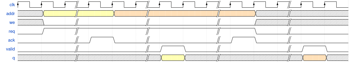
The SDRAM controller allows read operations to be performed using a simple interface.

Read requests can be chained so that a new read operation can be requested before the current operation has completed. Using this strategy, we can read any number of words from the SDRAM without wasting clock cycles, thus using the maximum available bandwidth of the SDRAM.

The following example describes how to read two 32-bit words using the SDRAM controller. This method can be used to read any number of words:

  1. Write the address to the addr bus.
  2. Request a read operation by deasserting the we signal and asserting the req signal.
  3. Wait for the ack signal to be asserted. This means that the read request has been acknowledged, and a read operation has begun.
  4. Write another address to the addr bus.
  5. Wait for the valid signal to be asserted. This means that the first read request has been completed and the data is available on the data bus.
  6. Read the value on the q data bus.
  7. Wait for ack signal to be asserted. This means that the second read request has been acknowledged, and a read operation has begun.
  8. Deassert the req signal when we're done making requests.
  9. Wait for the valid signal to be asserted. This means that the second read request has been completed and the data is available on the data bus.
  10. Read the value on the q data bus.

SDRAM Controller Read

Writing

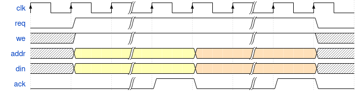
The SDRAM controller handles write operations similarly to read operations.

Write requests can also be chained, so that a new write operation can be requested before the current operation has completed.

The following example describes how to write two 32-bit words using the SDRAM controller. This method can be used to write any number of words:

  1. Write an address to the addr bus and a value to the data bus.
  2. Request a write operation by asserting the we and req signals.
  3. Wait for the ack signal to be asserted. This means that the write request has been acknowledged, and a write operation has begun.
  4. Write another address to the addr bus and a value to the data bus.
  5. Wait for ack signal to be asserted. This means that the second write request has been acknowledged, and a write operation has begun.
  6. Deassert the we and req signals when we're done making requests.

SDRAM Controller Write

State Diagram

State Diagram

Licence

This project is licensed under the MIT licence. See the LICENCE file for more details.

sdram-fpga's People

Contributors

nullobject avatar

Stargazers

 avatar  avatar  avatar  avatar  avatar  avatar  avatar  avatar  avatar  avatar  avatar  avatar  avatar  avatar  avatar  avatar  avatar  avatar  avatar  avatar  avatar  avatar  avatar  avatar  avatar  avatar  avatar  avatar  avatar  avatar  avatar  avatar  avatar  avatar  avatar  avatar  avatar  avatar  avatar  avatar  avatar  avatar  avatar  avatar  avatar  avatar  avatar  avatar  avatar  avatar  avatar  avatar  avatar  avatar  avatar  avatar  avatar  avatar  avatar  avatar  avatar  avatar  avatar  avatar  avatar  avatar  avatar  avatar  avatar  avatar  avatar  avatar  avatar  avatar  avatar  avatar  avatar  avatar  avatar  avatar  avatar  avatar  avatar  avatar  avatar  avatar  avatar  avatar  avatar  avatar  avatar  avatar  avatar  avatar  avatar  avatar  avatar  avatar  avatar  avatar

Watchers

 avatar  avatar  avatar  avatar  avatar  avatar  avatar  avatar  avatar  avatar  avatar  avatar  avatar  avatar  avatar

sdram-fpga's Issues

Why add data again in the second burst write?

Write an address to the addr bus and a value to the data bus.
Request a write operation by asserting the we and req signals.
Wait for the ack signal to be asserted. This means that the write request has been acknowledged, and a write operation has begun.
Write another address to the addr bus and a value to the data bus.
Wait for ack signal to be asserted. This means that the second write request has been acknowledged, and a write operation has begun.
Deassert the we and req signals when we're done making requests.

Hi, Josh thanks for this controller. I have a question for the bold lines.
Since I understand the first step is to set the address(22 in my case 2BANK-12ROW-8COLUMN) and the data bus(32). Since it's in 2 burst mode, the first 16 bits are written in the address, once ack is rised it says that I need to set again a new address and ¿new data? what about the 16 bits left? Can u help me in that?

Thanks for the answer!

New to VHDL

the code here im trying to use this, but i have no idea where to start
i've added the single file to project file.
but i have a different TOP file.

when using component, non of the physical pins are registered and doesnt synthesise

TOP_MAIN.vhdl
SDRAM.vhdl
SDRAMPLL.vhdl

how would i go about this??
thanks

Read @Burstlenght > 2

Hi,

to save more than the default numbers of words (BURST_LENGTH == 2) i did the following modification @ process "latch_sdram_data"

signal word_cnt_int : natural range 0 to BURST_LENGTH-1;

if first_word = '1' then
q_reg(DATA_WIDTH-1 downto DATA_WIDTH-SDRAM_DATA_WIDTH) <= sdram_dq;
word_cnt_int <= 1; --initwert
elsif read_done = '1' then
q_reg(SDRAM_DATA_WIDTH-1 downto 0) <= sdram_dq;
valid <= '1';
elsif word_cnt_int > 0 then -- 2. Word....
q_reg(DATA_WIDTH-1 - word_cnt_intSDRAM_DATA_WIDTH downto DATA_WIDTH - word_cnt_intSDRAM_DATA_WIDTH -SDRAM_DATA_WIDTH) <= sdram_dq;
word_cnt_int <= word_cnt_int+1;
end if;

-- if first_word = '1' then
-- q_reg(31 downto 16) <= sdram_dq;
-- elsif read_done = '1' then
-- q_reg(15 downto 0) <= sdram_dq;
-- valid <= '1';
-- end if;

Add support for data byte select signals

Currently the sdram_dqmh and sdram_dqml signals are hard-wired to zero. I assume that these two signals can be used for implementing "byte select" during write operations.

For my application (a custom soft CPU with 8/16/32-bit word writing capabilities), byte select functionality in the SDRAM controller would simplify the interface significantly (otherwise I'd need to do a full 32-bit read-modify-write cycle to support writing of individual bytes, for instance).

Would it be hard to implement?

long sequential read burst

HI

For video framebuffer to optimize RAM bandwidth and allow
higher display resolution, some sequential read bursts of 1-2K
from RAM would mean much. If you have some plans or will to make,
it, I'd volunteer for testing :)

Errors - what software / version is needed to compile this?

I've tried to get this to compile in Quartus Prime Lite 15.1.0, but I get errors.

What software/version is this intended to be compiled by?

The first error was:

Error (10481): VHDL Use Clause error at sdram.vhd(26): design library "work" does not contain primary unit "common". Verify that the primary unit exists in the library and has been successfully compiled.

So, I tried adding

library work;

which didn't help, so I tried commenting out the line for use work.common.all;, which led to the next error:

Error (10482): VHDL error at sdram.vhd(140): object "ilog2" is used but not declared

It seems knowing the actual software version (e.g. of Quartus) is necessary to get almost anything to compile. Maybe I'm missing it, but I don't see that mentioned.

Frequency caclulation seems wrong

Does this math add up? At the start of the module we have:
entity sdram is
generic (
-- clock frequency (in MHz)
--
-- This value must be provided, as it is used to calculate the number of
-- clock cycles required for the other timing values.
CLK_FREQ : real;

Then later on:
-- calculate the clock period (in nanoseconds)
constant CLK_PERIOD : real := 1.0/CLK_FREQ*1000.0;

But if for example we pass CLK_FREQ = 100.0 which is 100MHZ then the period in ns is calculated as 1/100*1000=0.00001ns

Did you meant to say instead:
constant CLK_PERIOD : real := 1000.0/CLK_FREQ;

Can I use two 16x8 chips in parallel?

I only have 16x8 parts available from old dual bank ram modules. I'd very much like to recycle old hardware instead of buying new parts. Is it possible?

Cheers!

Recommend Projects

  • React photo React

    A declarative, efficient, and flexible JavaScript library for building user interfaces.

  • Vue.js photo Vue.js

    🖖 Vue.js is a progressive, incrementally-adoptable JavaScript framework for building UI on the web.

  • Typescript photo Typescript

    TypeScript is a superset of JavaScript that compiles to clean JavaScript output.

  • TensorFlow photo TensorFlow

    An Open Source Machine Learning Framework for Everyone

  • Django photo Django

    The Web framework for perfectionists with deadlines.

  • D3 photo D3

    Bring data to life with SVG, Canvas and HTML. 📊📈🎉

Recommend Topics

  • javascript

    JavaScript (JS) is a lightweight interpreted programming language with first-class functions.

  • web

    Some thing interesting about web. New door for the world.

  • server

    A server is a program made to process requests and deliver data to clients.

  • Machine learning

    Machine learning is a way of modeling and interpreting data that allows a piece of software to respond intelligently.

  • Game

    Some thing interesting about game, make everyone happy.

Recommend Org

  • Facebook photo Facebook

    We are working to build community through open source technology. NB: members must have two-factor auth.

  • Microsoft photo Microsoft

    Open source projects and samples from Microsoft.

  • Google photo Google

    Google ❤️ Open Source for everyone.

  • D3 photo D3

    Data-Driven Documents codes.