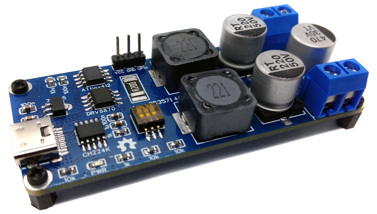
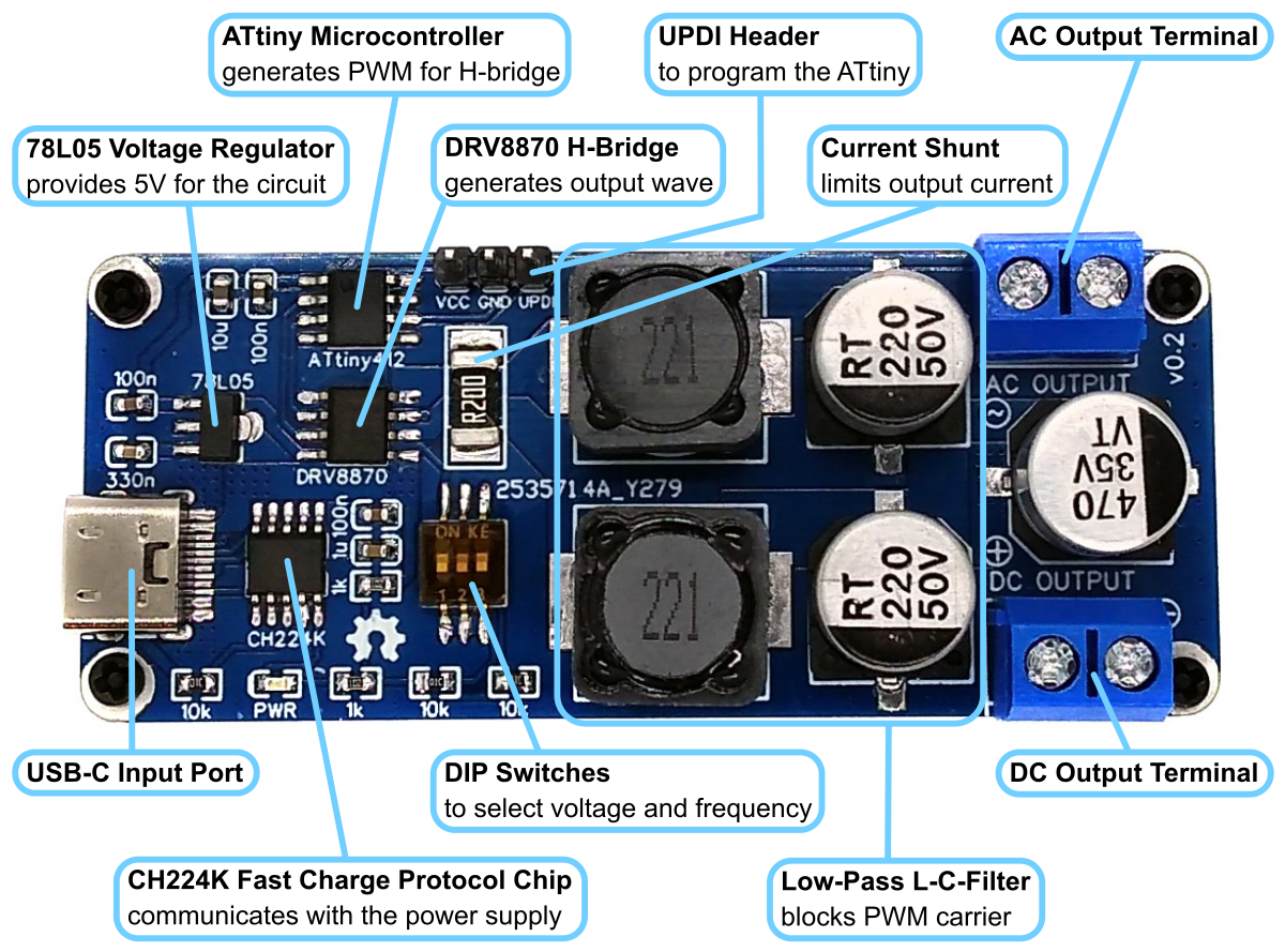
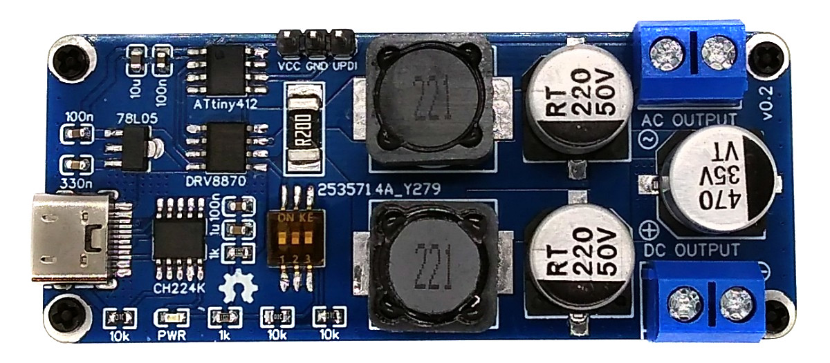
The ATtiny212/412-based USB Power Delivery Inverter converts direct current from USB PD power supplies into sine wave alternating current with selectable voltage and adjustable frequency. For this purpose, the ATtiny's powerful Timer/Counter D (TCD) controls an H-Bridge with a subsequent low-pass filter.
- Design Files (EasyEDA): https://oshwlab.com/wagiminator/attiny412-usb-pd-inverter
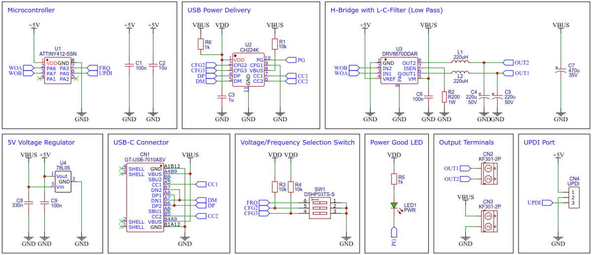
The 78L05 is a simple and inexpensive voltage regulator that can convert input voltages up to 30V to an output voltage of 5V with an output current of up to 200mA and a dropout voltage of 1.7V. The 78L05 supplies some elements of the circuit with 5V.
The CH224K is a USB PD power receiving protocol chip, which integrates PD3.0/2.0, BC1.2 and other fast charging protocols, automatically detects VCONN and analog E-Mark chips, supports up to 100W power, and has built-in PD communication module. It also integrates output voltage detection internally to support overheating and overvoltage protection. It features:
- 4V to 22V input voltage
- PD3.0/2.0, BC1.2 and other fast charging protocols
- USB Type-C PD, positive and negative insertion detection and automatic switching
- E-Mark simulation, automatically detects VCONN, supports 100W power PD request
- requested voltage can be dynamically adjusted through a variety of methods
- high integration of single chip, simplified peripheral and low cost
- built-in over-voltage and over-temperature protection module
In this application, the CH224K is used to communicate with the USB PD Power Adapter to request the output voltage selected via the DIP switches. The CH224K's PG pin is open-drain, pulling the input to ground when the requested voltage has been successfully negotiated with the USB PD power supply. Here it is used to drive an indicator LED.
The DRV8870 device is a brushed-DC motor driver for printers, appliances, industrial equipment, and other small machines. Two logic inputs control the H-bridge driver, which consists of four N-channel MOSFETs that can control motors bidirectionally with up to 3.6A peak current. The inputs can be pulsewidth modulated (PWM) to control motor speed, using a choice of current-decay modes. Setting both inputs low enters a low-power sleep mode. It features:
- H-Bridge Motor Driver
- Wide 6.5-V to 45-V Operating Voltage
- 565-mΩ Typical RDS(on) (HS + LS)
- 3.6A Peak Current Drive
- PWM Control Interface
- Integrated Current Regulation
- Low-Power Sleep Mode
- Small Package and Footprint
- Integrated Protection Features
- VM Undervoltage Lockout (UVLO)
- Overcurrent Protection (OCP)
- Thermal Shutdown (TSD)
- Automatic Fault Recovery
In this application, the H-bridge is used to switch the polarity of the input voltage with high frequency PWM and a variable duty cycle. A downstream low-pass L-C filter removes the original high-frequency PWM signal, leaving only the lower-frequency sine wave modulated via the duty cycle at the output. The cutoff frequency of the filter should be well between the PWM freqency (19kHz) and the sine wave frequency (50Hz or 60Hz). The cutoff frequency depending on the inductor (L1, L2) and capacitor (C4, C5) can be determined using the following formula:
The DRV8870 offers the possibility to set a current limit via a resistor (R2). The resistance value is calculated as follows:
The ATtiny212 or ATtiny412 microcontroller generates the high-frequency PWM signal with the duty cycle modulated sine wave for the H-bridge.
Two complementary logic signals with intermediate dead times (break-before-make times) are required to control the H-bridge. The dead times are necessary to prevent short circuits due to H-bridge switching delays. To generate this, the ATtiny's powerful Timer/Counter D (TCD) is used, which is also specialized in controlling H-bridges, among other things. The TCD is operated in Four Ramp Mode with a clock frequency of
In Four Ramp mode, the TCD cycle follows this pattern:
- A TCD cycle begins with the TCD counter counting up from zero until it reaches the CMPASET value. Then it resets to zero and switches the WOA pin to HIGH.
- The counter counts up until it reaches the CMPACLR value, then it resets to zero and switches the WOA pin to LOW.
- The counter counts up until it reaches the CMPBSET value, then it resets to zero and switches the WOB pin to HIGH.
- The counter counts up until it reaches the CMPBCLR value, and ends the TCD cycle by resetting to zero and switching WOB pin to LOW.
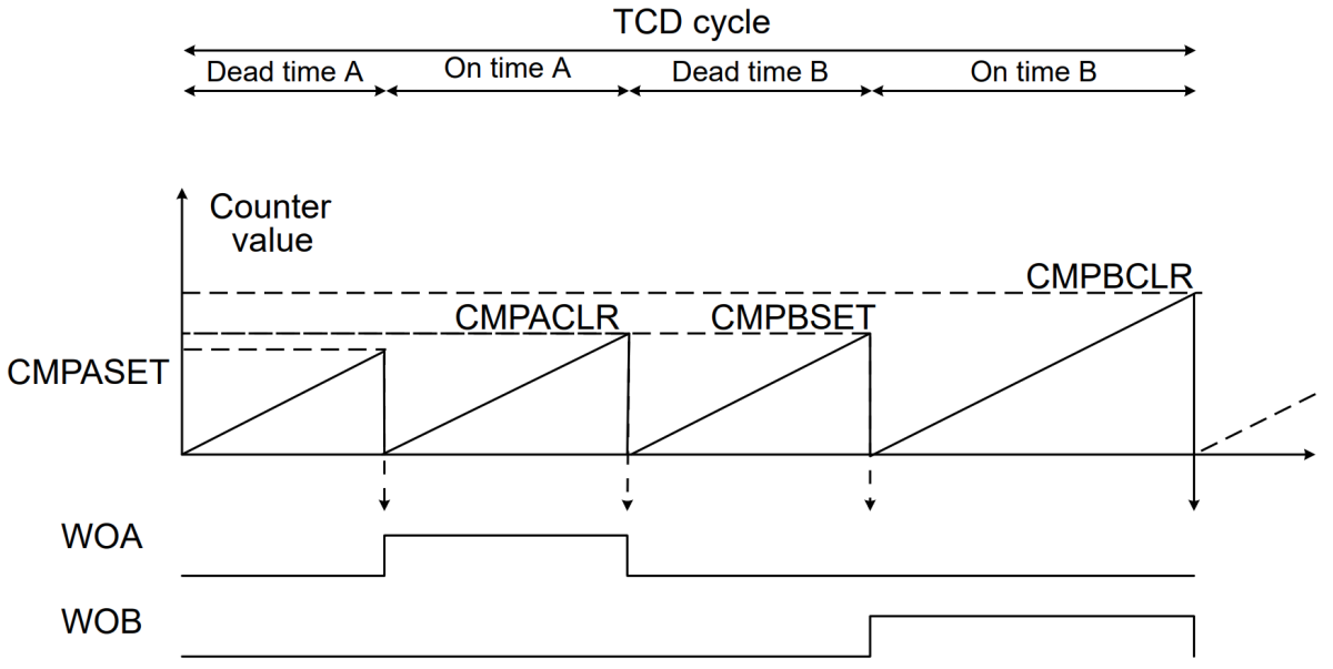
The values of the registers CMPASET and CMPBSET determine the length of the respective dead times. At the beginning, these are set in such a way that they are each 200ns and are then not changed any more.
int main(void) {
  _PROTECTED_WRITE(CLKCTRL.MCLKCTRLB, 0);     // set clock frequency to 20 MHz
  pinOutput(PIN_WOA); pinOutput(PIN_WOB);     // enable output on WOA/WOB pin
  TCD0.CTRLB     = TCD_WGMODE_FOURRAMP_gc;    // set four ramp mode
  TCD0.CMPASET   = 0x00;                      //   200ns dead time
  TCD0.CMPACLR   = 0x80;                      // 25800ns on-time WOA
  TCD0.CMPBSET   = 0x00;                      //   200ns dead time
  TCD0.CMPBCLR   = 0x7f;                      // 25600ns on-time WOB
  CPU_CCP        = CCP_IOREG_gc;              // protected write is coming
  TCD0.FAULTCTRL = TCD_CMPAEN_bm              // enable WOA output channel
                 | TCD_CMPBEN_bm;             // enable WOB output channel
  TCD0.INTCTRL   = TCD_OVF_bm;                // enable overflow interrupt
  while(~TCD0.STATUS & TCD_ENRDY_bm);         // wait for synchronization
  TCD0.CTRLA     = TCD_CLKSEL_20MHZ_gc        // select 20MHz base clock
                 | TCD_CNTPRES_DIV4_gc        // prescaler 4 -> 5MHz timer clock
                 | TCD_ENABLE_bm;             // enable timer
  sei();                                      // enable interrupts
  while(1);                                   // everything is done via interrupt
}
CMPACLR determines the length of the WOA/IN1 signal, CMPBCLR the length of the WOB/IN2 signal for the H-bridge. Both lengths are changed after each TCD cycle according to a sine table and are always complementary to each other. This is controlled via the TCD overflow interrupt, which calls the appropriate interrupt service routine at the end of each TCD cycle:
ISR(TCD0_OVF_vect) {
  TCD0.CMPACLRL =  SIN_val;                   // set next sine value for WOA
  TCD0.CMPBCLRL = -SIN_val;                   // inverse value for WOB
  TCD0.CTRLE    = TCD_SYNCEOC_bm;             // sync registers at TCD cycle end
  TCD0.INTFLAGS = TCD_OVF_bm;                 // clear interrupt flag
  if(++SIN_ptr >= sizeof(SIN)) SIN_ptr = 0;   // increase sine pointer
  SIN_val = SIN[SIN_ptr];                     // get next sine value
}
This results in a PWM signal with always the same length and the same dead times, but a variable duty cycle. The period of the TCD cycle and thus the length of the PWM signal is calculated as follows:
Since the amplitude of the sine table was chosen so that the values are between 0 and 255, CMPACLR and CMPBCLR are always complementary (CMPACLR + CMPBCLR = 255) and CMPASET = CMPBSET = 0, this results in a TCD period of 259 clock cycles or 51.8µs. The PWM frequency is calculated as follows:
The number of values in the sine table for a complete period determines the frequency of the sine wave. It is calculated as follows:
So the frequency of the output voltage can be controlled, among other things, by the number of values in the sine table. The AC output voltage itself is determined by the DC input voltage and the amplitude of the sine wave in the table. Since this oscillates fully from 0 to 255 here, the AC output voltage (RMS) is calculated as follows:
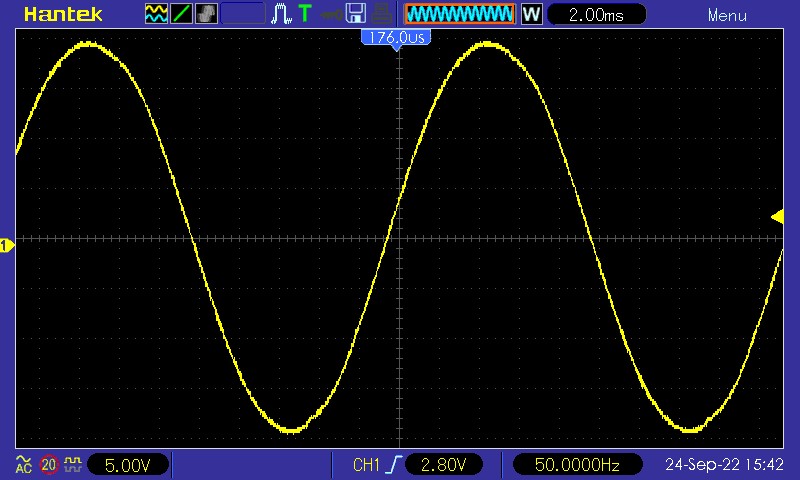
Here's the final wave at the AC output terminal:
- Open your Arduino IDE.
- Make sure you have installed megaTinyCore.
- Go to Tools -> Board -> megaTinyCore and select ATtiny412/402/212/202.
- Go to Tools and choose the following board options:
- Chip: ATtiny212 or ATtiny412
- Clock: 20 MHz internal
- Leave the rest at the default settings.
- Connect your programmer to your PC and to the UPDI header on the board.
- Go to Tools -> Programmer and select your UPDI programmer.
- Go to Tools -> Burn Bootloader to burn the fuses.
- Open the sketch and click Upload.
- Connect your programmer to your PC and to the UPDI header on the board.
- Make sure you have installed the latest avr-gcc toolchain.
- Open a terminal.
- Navigate to the folder with the makefile and the sketch.
- Run
DEVICE=attiny412 PROGRMR=serialupdi PORT=/dev/ttyUSB0 make installto compile, burn the fuses and upload the firmware (change DEVICE, PROGRMR and PORT accordingly).
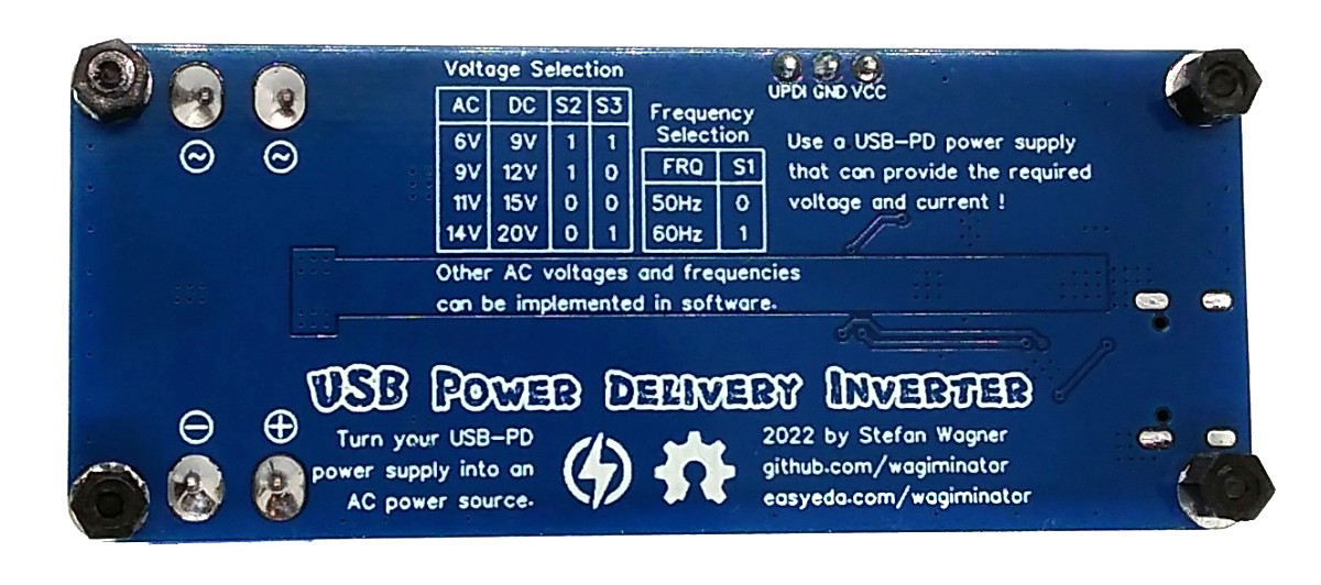
Use the DIP switches on the device to select the output voltage and AC frequency. Connect the device to a USB PD power adapter. As soon as the LED lights up, the correct output values are present. The switch positions can also be changed during operation.
The output voltage is selected via two of the three DIP switches according to the following table:
| DC Voltage | AC Voltage | SW2 | SW3 |
|---|---|---|---|
| 9V | 6.4V | 1 | 1 |
| 12V | 8.5V | 1 | 0 |
| 15V | 10.6V | 0 | 0 |
| 20V | 14.1V | 0 | 1 |
The AC output frequency is selected via the first DIP switch as follows:
| Frequency | SW1 |
|---|---|
| 50Hz | 0 |
| 60Hz | 1 |
- 78L05 Datasheet
- CH224K Datasheet
- DRV8870 Datasheet
- ATtiny412 Datasheet
- Sine Table Generator
- CH224K USB PD Adapter
- CH224K USB PD Decoy
- IP6520 USB PD Source
- TI Primer on USB PD

This work is licensed under Creative Commons Attribution-ShareAlike 3.0 Unported License. (http://creativecommons.org/licenses/by-sa/3.0/)


