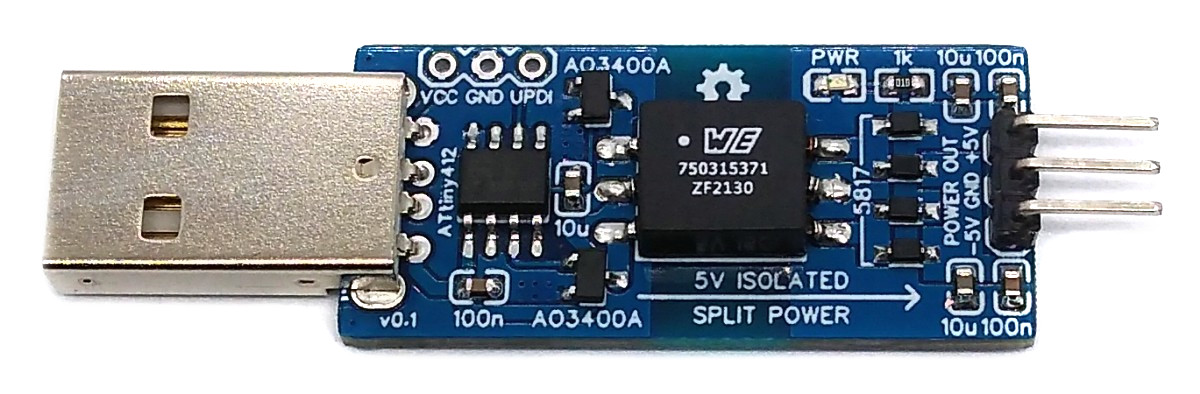
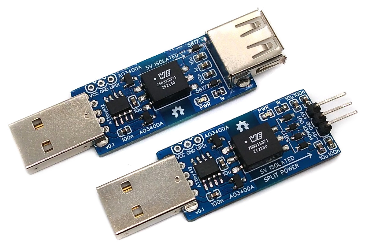
For some applications, a galvanically isolated power supply is required to avoid ground loops or short circuits, or simply for mutual protection. The USB Power Isolator offers the possibility of a simple isolation (2.5kV) of the 5V rail of a USB power adapter with an unregulated output and a maximum continuous current of 1A. The USB Power Isolator isolates the power rail only, for full isolation including data lines take a look at the ADuM3160 USB Isolator.
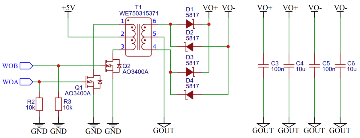
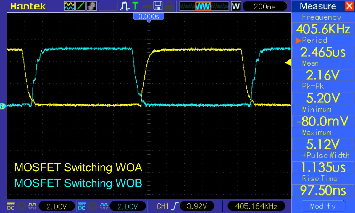
Using its powerful Timer/Counter D (TCD), the ATtiny212/412 controls a center-tapped transformer utilizing the push-pull topology by providing complementary output signals with intermediate dead times (break-before-make time) to drive the two ground-referenced N-channel MOSFETs connected to the transformer's outer taps and alternately turn them on and off. The implemented switching frequency of 400kHz is specially tailored to the Würth Elektronik 750315371 transformer, but other frequencies and features like spread spectrum clocking can be implemented in software if required.
There are actually special ICs to drive push-pull transformers, in the case of the WE750315371 this is for example the SN6505B. However, the small ATtinys are significantly cheaper and can easily imitate the tasks of these ICs.
Push-pull converters require center-tapped transformers to transfer power from the primary to the secondary. The way it works is clearly described in the SN6505B datasheet.
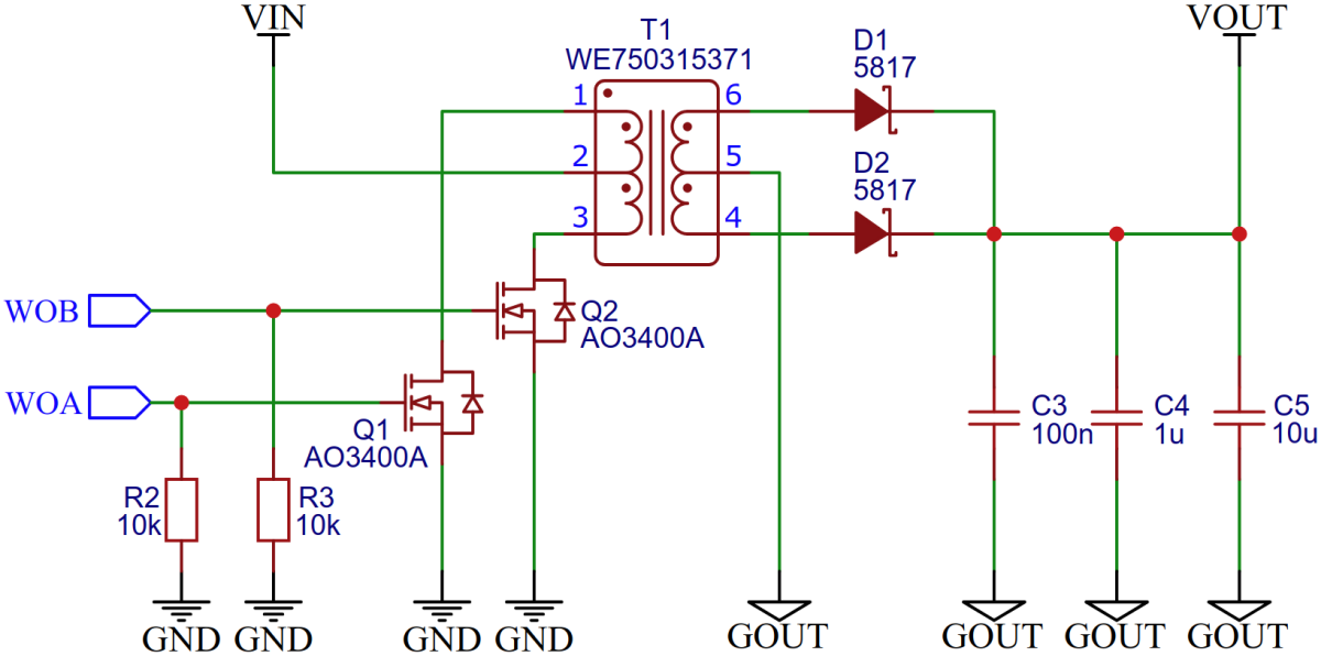
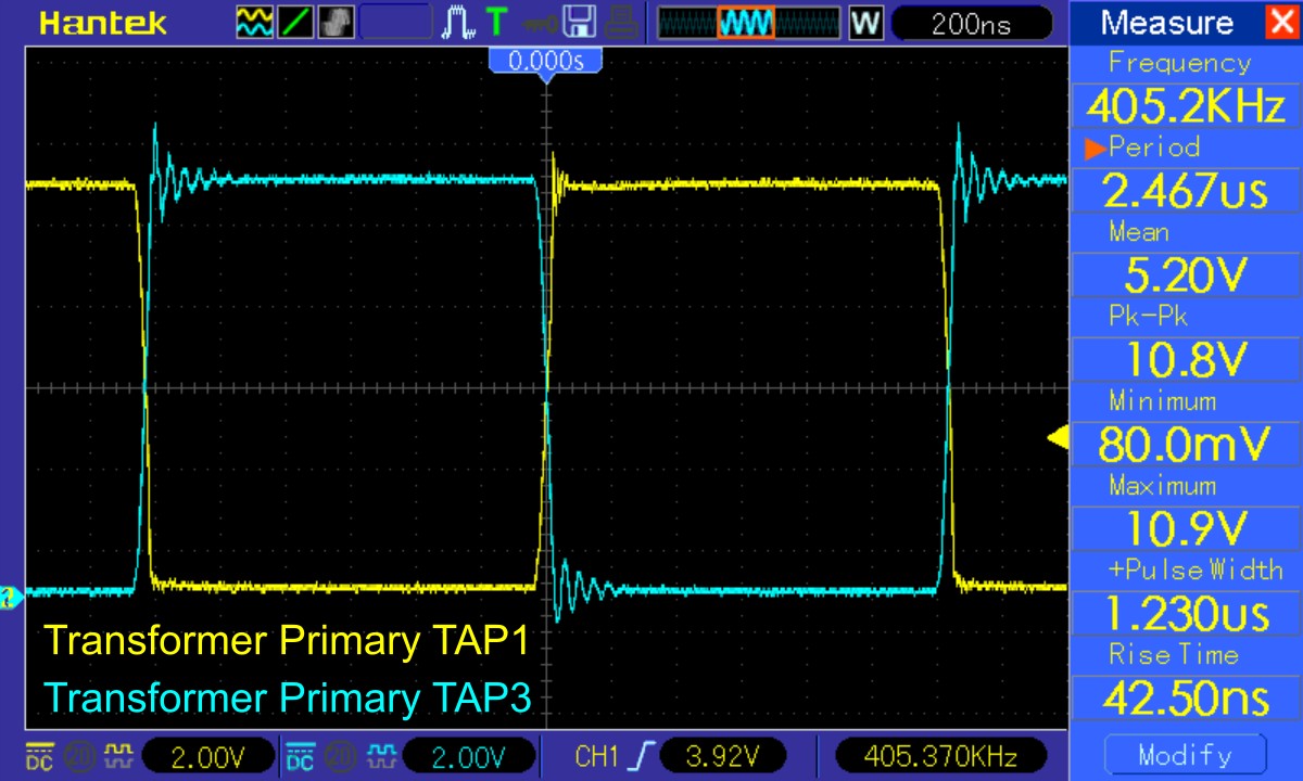
When Q1 conducts, VIN (+5V) drives a current through the upper half of the primary to ground, thus creating a negative voltage potential at the upper primary end with regards to the VIN potential at the center-tap.
At the same time the voltage across the lower half of the primary is such that the lower primary end is positive with regards to the center-tap in order to maintain the previously established current flow through Q2, which now has turned high-impedance. The two voltage sources, each of which equaling VIN (+5V), appear in series and cause a voltage potential at the open end of the primary of 2×VIN (+10V) with regards to ground.
Per dot convention the same voltage polarities that occur at the primary also occur at the secondary. The positive potential of the lower secondary end therefore forward biases diode D2. The secondary current starting from the lower secondary end flows through D2, charges capacitors C3 - C5, and returns through the load impedance back to the center-tap.
When Q2 conducts, Q1 goes high-impedance and the voltage polarities at the primary and secondary reverse. Now the upper end of the primary presents the open end with a 2×VIN (+10V) potential against ground. In this case D1 is forward biased while D2 is reverse biased and current flows from the upper secondary end through D1, charging the capacitors and returning through the load to the center-tap.
The choice of a suitable center-tapped transformer essentially depends on the input voltage, the output voltage, the current and the switching frequency.
To prevent a transformer from saturating, its voltage-time product (V-t product) must be greater than the maximum V-t product applied by the device. The maximum voltage supplied by the device is the nominal input voltage (here
Common V-t values for low-power, center-tapped transformers range from 22Vμs to 150Vμs in typical 10mm x 12mm footprints. However, transformers specifically designed for PCMCIA applications only deliver 11Vμs and have a significantly reduced footprint of just 6mm x 6mm. According to the data sheet, the WE750315371 transformer used here has a V-t product of 8.6Vμs for bipolar operation. Since the switching frequency can be changed in software, transformers with other V-t values can also be used.
Although V-t-wise all of these transformers can be driven by the device, other important factors such as isolation voltage, transformer rating and turns ratio must be considered before making the final decision. To calculate the turns ratio of the transformer, the efficiency of the transformer, the desired output voltage, the voltage drop at the diodes and the MOSFETs as well as the dropout voltage of the linear regulator that may be connected downstream are important.
The 1N5817 Schottky diodes used here have a forward voltage drop of
The WE750315371 transformer used here has a turns ratio of 1.1 (±2%), so that fits.
An N-channel MOSFET with a gate threshold voltage
When choosing the diodes, Schottky diodes with the lowest possible forward voltage
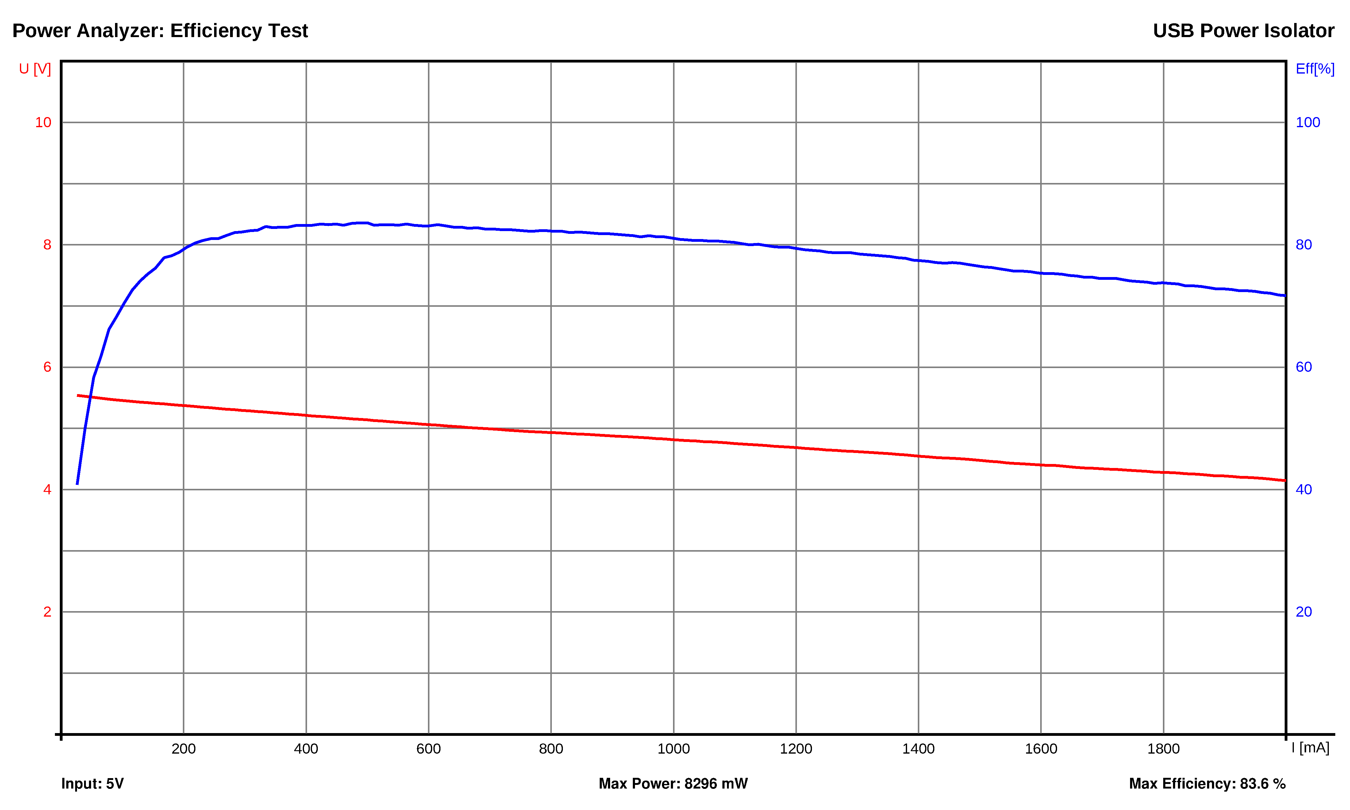
The USB Power Isolator has an unregulated output, which means that the output voltage depends significantly on the input voltage and the current drawn. In order to stabilize the output voltage, a linear voltage regulator can be connected downstream if required. A voltage regulator with the lowest possible dropout voltage
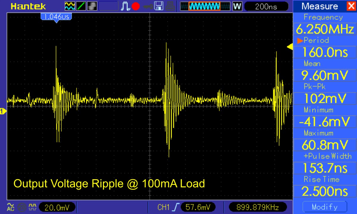
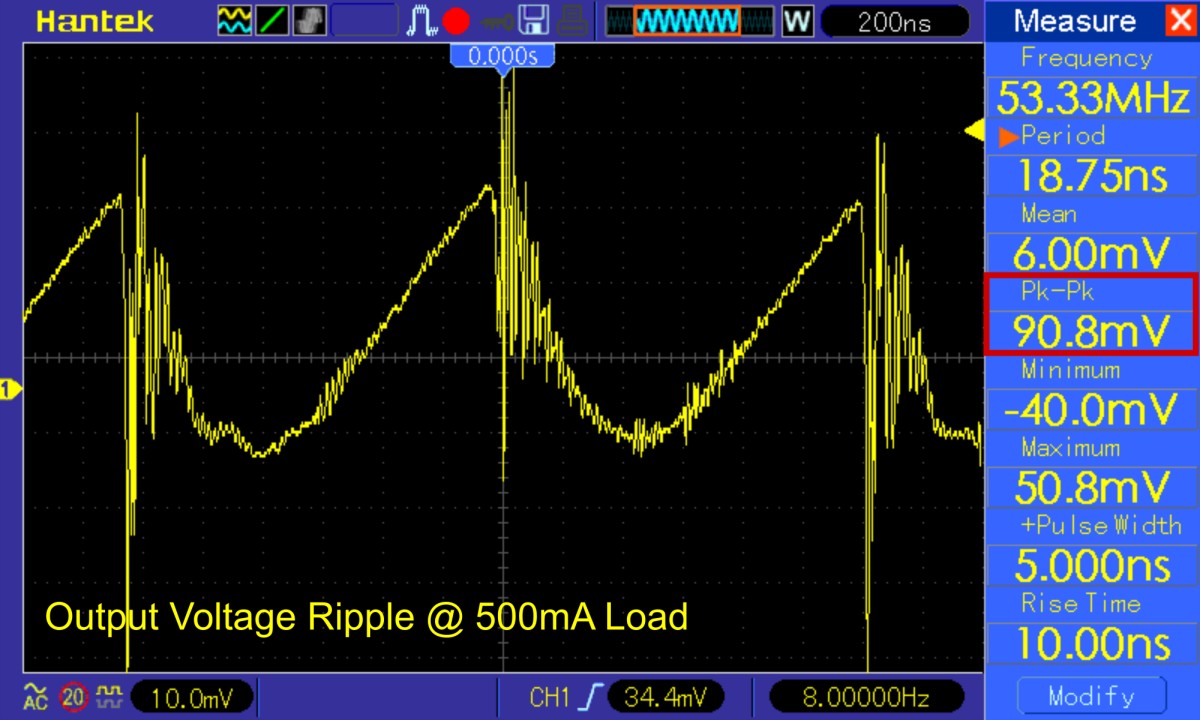
Switching converters cause ripple at the output voltage due to their functional principle. The output capacitors C3 - C5 smooth this out somewhat, but by no means completely. A much clearer smoothing can be achieved by a downstream L-C low-pass filter, which consists of an inductor and a capacitor.
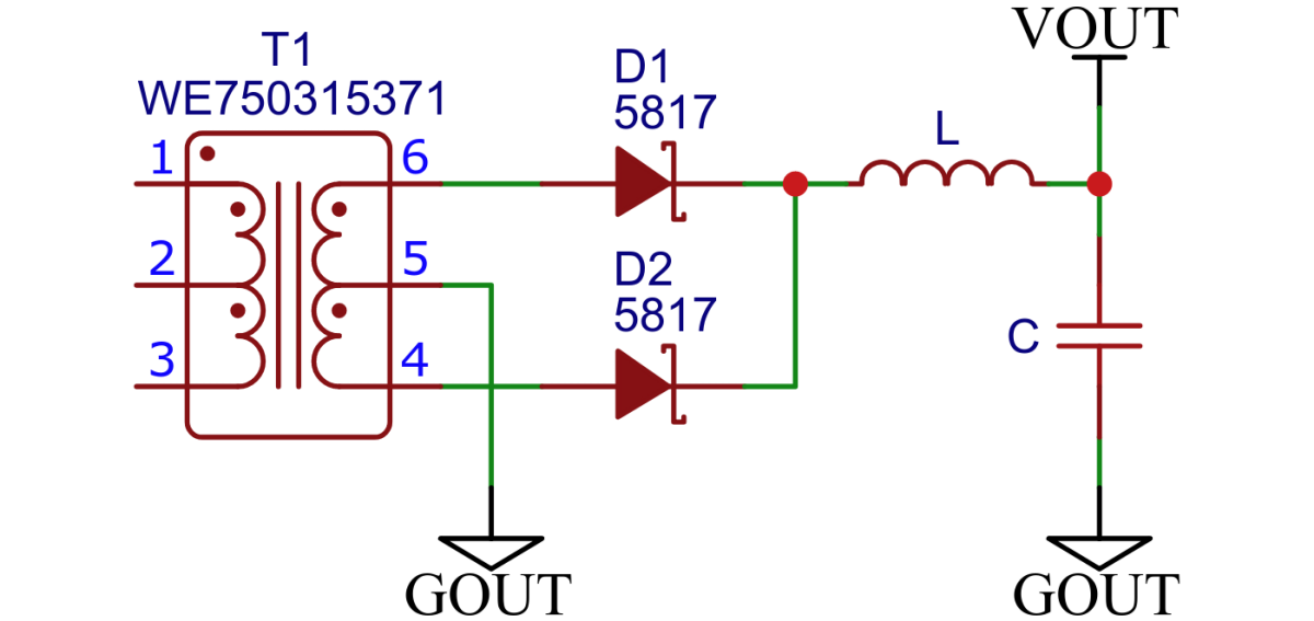
It is important to ensure that the inductor can withstand the maximum output current
The lower the cut-off frequency of the filter, the better its ripple reduction effect. This can be achieved with a larger inductance and/or a larger capacitance.
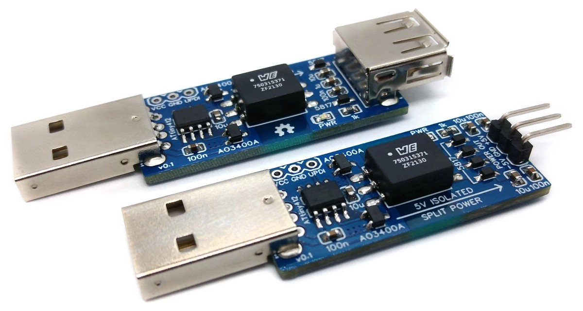
Two PCB implementations are available. The first outputs unregulated 5V via a female USB socket and can be easily plugged in between the USB power adapter and the consumer. The second can be used as a split power supply with +5V and -5V.
- Design Files (EasyEDA): https://oshwlab.com/wagiminator/attiny412-5v-isolated-dc-dc-converter
- Design Files (EasyEDA): https://oshwlab.com/wagiminator/attiny412-5v-isolated-dual-supply
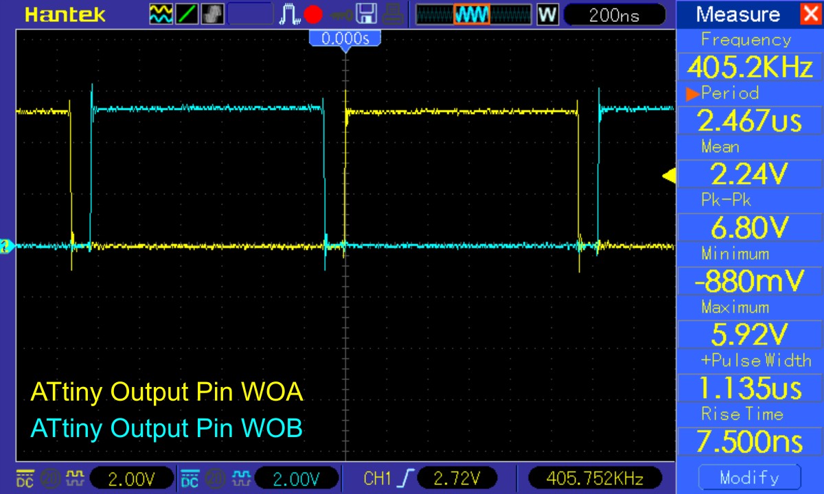
Two complementary logic signals with intermediate dead times (break-before-make times) are required to control the gates of the two MOSFETs, which are switched on and off alternately. Before either one of the gates can assume logic high, the dead time logic ensures a short time period during which both signals are low and both MOSFETs are high-impedance. This short period is required to avoid shorting out both ends of the primary. The ATtiny's Timer/Counter D (TCD) is used to generate these signals.
The TCD is operated in Four Ramp Mode with a clock frequency of 20MHz. The two outputs WOA and WOB drive the gates of the two MOSFETs which are connected to the outer taps of the primary side of the transformer.
In Four Ramp mode, the TCD cycle follows this pattern:
- A TCD cycle begins with the TCD counter counting up from zero until it reaches the CMPASET value. Then it resets to zero and switches the WOA pin to HIGH.
- The counter counts up until it reaches the CMPACLR value, then it resets to zero and switches the WOA pin to LOW.
- The counter counts up until it reaches the CMPBSET value, then it resets to zero and switches the WOB pin to HIGH.
- The counter counts up until it reaches the CMPBCLR value, and ends the TCD cycle by resetting to zero and switching WOB pin to LOW.
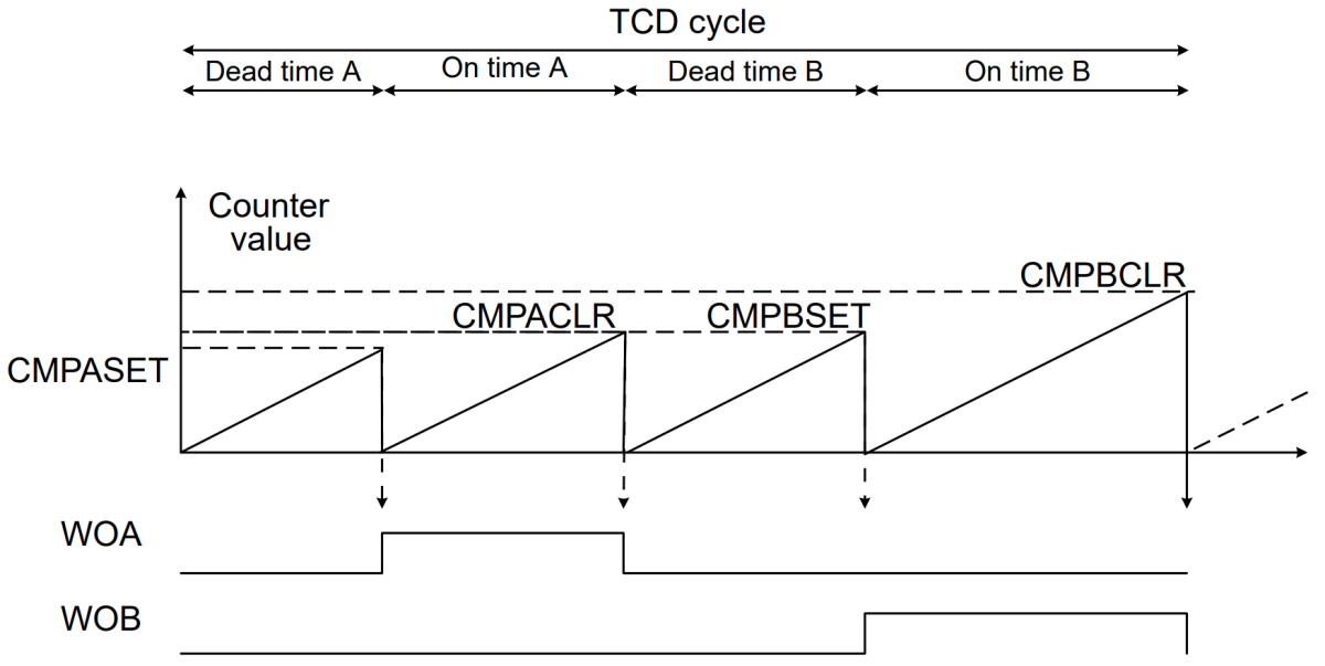
The values of the registers CMPASET and CMPBSET determine the length of the respective dead times, registers CMPACLR and CMPBCLR the on times of WOA and WOB, respectively. Both dead times and both on times must be the same in each case so that an imbalance in the magnetic flux density swing is avoided and the transformer does not creep into the saturation region.
A dead time of
The length of the on times can be calculated from the length of the switching period and the length of the dead times:
Since the TCD works with a clock frequency of
The main function of the firmware is thus as follows:
int main(void) {
  _PROTECTED_WRITE(CLKCTRL.MCLKCTRLB, 0);         // set clock frequency to 20 MHz
  pinOutput(PIN_WOA); pinOutput(PIN_WOB);         // enable output on WOA/WOB pin
  TCD0.CTRLB     = TCD_WGMODE_FOURRAMP_gc;        // set TCD four ramp mode
  TCD0.CMPASET   = 01;                            //  100ns dead time
  TCD0.CMPACLR   = 22;                            // 1150ns on-time WOA
  TCD0.CMPBSET   = 01;                            //  100ns dead time
  TCD0.CMPBCLR   = 22;                            // 1150ns on-time WOB
  CPU_CCP        = CCP_IOREG_gc;                  // protected write is coming
  TCD0.FAULTCTRL = TCD_CMPAEN_bm                  // enable WOA output channel
                 | TCD_CMPBEN_bm;                 // enable WOB output channel
  while(~TCD0.STATUS & TCD_ENRDY_bm);             // wait for synchronization
  TCD0.CTRLA     = TCD_CLKSEL_20MHZ_gc            // select 20MHz base clock
                 | TCD_CNTPRES_DIV1_gc            // no prescaler -> 20MHz TCD clock
                 | TCD_ENABLE_bm;                 // enable timer
  SLPCTRL.CTRLA  = SLPCTRL_SMODE_IDLE_gc          // set sleep mode to IDLE
                 | SLPCTRL_SEN_bm;                // enable sleep
  while(1) sleep_cpu();                           // CPU is not needed anymore
}- Open your Arduino IDE.
- Make sure you have installed megaTinyCore.
- Go to Tools -> Board -> megaTinyCore and select ATtiny412/402/212/202.
- Go to Tools and choose the following board options:
- Chip: ATtiny212 or ATtiny412
- Clock: 20 MHz internal
- Leave the rest at the default settings.
- Connect your programmer to your PC and to the UPDI header on the board.
- Go to Tools -> Programmer and select your UPDI programmer.
- Go to Tools -> Burn Bootloader to burn the fuses.
- Open the sketch and click Upload.
- Connect your programmer to your PC and to the UPDI header on the board.
- Make sure you have installed the latest avr-gcc toolchain.
- Open a terminal.
- Navigate to the folder with the makefile and the sketch.
- Run
DEVICE=attiny412 PROGRMR=serialupdi PORT=/dev/ttyUSB0 make installto compile, burn the fuses and upload the firmware (change DEVICE, PROGRMR and PORT accordingly).
| Parameter | Value |
|---|---|
| Input Voltage | 4.5 - 5.5V |
| Output Voltage | 4.7 - 5.5V |
| Output Voltage Ripple | 100mVpp@100mA |
| Output Current | max 1000mA |
| Standby Current | 35mA |
| Efficiency | max 83.6% |
| Isolation Voltage | 2500V |
- ATtiny412 Datasheet
- SN6505B Datasheet
- WE750315371 Datasheet
- AO3400A Datasheet
- 1N5817 Datasheet
- ADuM3160 USB Isolator

This work is licensed under Creative Commons Attribution-ShareAlike 3.0 Unported License. (http://creativecommons.org/licenses/by-sa/3.0/)


