zf3 / psram-tang-nano-9k Goto Github PK
View Code? Open in Web Editor NEWAn open source PSRAM/HyperRAM controller for Sipeed Tang Nano 9K / Gowin GW1NR-LV9QN88PC6/15 FPGA
License: Apache License 2.0
An open source PSRAM/HyperRAM controller for Sipeed Tang Nano 9K / Gowin GW1NR-LV9QN88PC6/15 FPGA
License: Apache License 2.0
Hi, I was attempting to simulate with iverilog, but I get
C:\code\psram-tang-nano-9k\src>iverilog -o top_tb.vvp psram_test_top.v
psram_test_top.v:200: error: Streaming concatenation requires SystemVerilog.
psram_test_top.v:201: error: Streaming concatenation requires SystemVerilog.
psram_test_top.v:202: error: Streaming concatenation requires SystemVerilog.
psram_test_top.v:203: error: Streaming concatenation requires SystemVerilog.
psram_test_top.v:204: error: Streaming concatenation requires SystemVerilog.
psram_test_top.v:205: error: Streaming concatenation requires SystemVerilog.
psram_test_top.v:206: error: Streaming concatenation requires SystemVerilog.
psram_test_top.v:207: error: Streaming concatenation requires SystemVerilog.
psram_test_top.v:215: error: Streaming concatenation requires SystemVerilog.
psram_test_top.v:216: error: Streaming concatenation requires SystemVerilog.
psram_test_top.v:217: error: Streaming concatenation requires SystemVerilog.
psram_test_top.v:218: error: Streaming concatenation requires SystemVerilog.
psram_test_top.v:219: error: Streaming concatenation requires SystemVerilog.
psram_test_top.v:220: error: Streaming concatenation requires SystemVerilog.
psram_test_top.v:221: error: Streaming concatenation requires SystemVerilog.
psram_test_top.v:222: error: Streaming concatenation requires SystemVerilog.
psram_test_top.v:223: error: Streaming concatenation requires SystemVerilog.

C:\code\psram-tang-nano-9k\src>iverilog -g2012 -o top_tb.vvp psram_test_top.v
psram_test_top.v:200: sorry: Streaming concatenation not supported.
psram_test_top.v:201: sorry: Streaming concatenation not supported.
psram_test_top.v:202: sorry: Streaming concatenation not supported.
psram_test_top.v:203: sorry: Streaming concatenation not supported.
psram_test_top.v:204: sorry: Streaming concatenation not supported.
psram_test_top.v:205: sorry: Streaming concatenation not supported.
psram_test_top.v:206: sorry: Streaming concatenation not supported.
psram_test_top.v:207: sorry: Streaming concatenation not supported.
psram_test_top.v:215: sorry: Streaming concatenation not supported.
psram_test_top.v:216: sorry: Streaming concatenation not supported.
psram_test_top.v:217: sorry: Streaming concatenation not supported.
psram_test_top.v:218: sorry: Streaming concatenation not supported.
psram_test_top.v:219: sorry: Streaming concatenation not supported.
psram_test_top.v:220: sorry: Streaming concatenation not supported.
psram_test_top.v:221: sorry: Streaming concatenation not supported.
psram_test_top.v:222: sorry: Streaming concatenation not supported.
psram_test_top.v:223: sorry: Streaming concatenation not supported.
I must admit I'm not particularly familiar with iverilog yet - I wonder if this should be simulatable with Icarus? Am I missing a proper command line directives, or would it be recommended to use some other simulator?
Thanks!
I got my exposure to Sipeed Tang Nano/Gowin PSRAM/HyperRAM first from this blog entry: https://justanotherelectronicsblog.com/?p=986
which links to this data sheet: https://www.winbond.com/resource-files/W956x8MBYA_64Mb_HyperBus_pSRAM_TFBGA24_datasheet_A01-003_20200724.pdf
The data sheet mentions both forms Differential Clock and Single Ended Clock, where it states:

Farther down in the document, it is stated that which one is used, is actually configurable via a register write:

That sounds interesting.
I find that in this repository, clock is not driven differentially signaled. There is a wire O_psram_ck_n defined as an input:
psram-tang-nano-9k/src/psram_test_top.v
Lines 13 to 14 in aa05c7b
but it is not referenced, so it will be swept in optimizing(?)
In the example code from justanotherelectronicsblog.com 's PSRAM controller, they also instantiate O_psram_ck_n:
but then drive it to constant low: https://github.com/riktw/tang4Kramblings/blob/215c2cea2204876a2993cfdfc43be37ccd4df9f7/NEORV32_HyperRAM/src/neorv32_test_setup_bootloader.vhd#L238
I have been trying to hack together a PSRAM test to Tang Nano 4K and 9K. In my test so far, I have got some serious stability issues if I try to increase the signaling clock speed beyond a few dozen MHz, and I wonder if it might be due to my buggy&hacky code, or due to some actual physical effects that would require Differential signaling to be enabled for the clock line.
I wonder if you have considered attempting to enable differential signaling for the clock line, or do you know if it makes any effect?
I also see that you have the project currently configured to run at 40.5 MHz - I'd be curious to know how far you have been able to push this speed?
Finally, one question: in this repo, I see you instantiate the HyperRAM IO via
psram-tang-nano-9k/src/psram_test_top.v
Lines 13 to 18 in aa05c7b
In my test code, which I think I have derived justanotherelectronicsblog.com, I instantiate it as follows:
  output [0:0] O_hpram_ck,      // HyperRAM Clock signal, ticks DDR (at both rising and falling edges)
  output [0:0] O_hpram_ck_n,    // Differential negative pair to O_hpram_ck signal. HyperRAM actually is configurable via a reg write whether to use differential signaling, and is disabled by default at boot.
  output [0:0] O_hpram_cs_n,    // Chip Select, active low.
  output [0:0] O_hpram_reset_n, // Reset, active low.
  inout  [7:0] IO_hpram_dq,     // 8-bit wide data path for CA (command & address) sends and data reads
  inout  [0:0] IO_hpram_rwds,   // Read-Write Data Strobe. Multiple purposes, see above.
I am not sure I understand the difference between these two. Since the DDR addressing clocks dq in and out every rising and falling edge, it seems that your code attempts to read/write 32-bits of data for every period of a rising+falling edge, whereas this code would only manage 16-bits per period. Have you tested if Tang Nano can actually write 32-bits of data for every rising+falling edge?
Thanks for publishing a really nice example code!
I spent at least a dozen hours learning Gowin FPGA PSRAM using your controller as an example. Nice job, thanks.
However I came across ambiguities while playing with Gowin Analyzer.
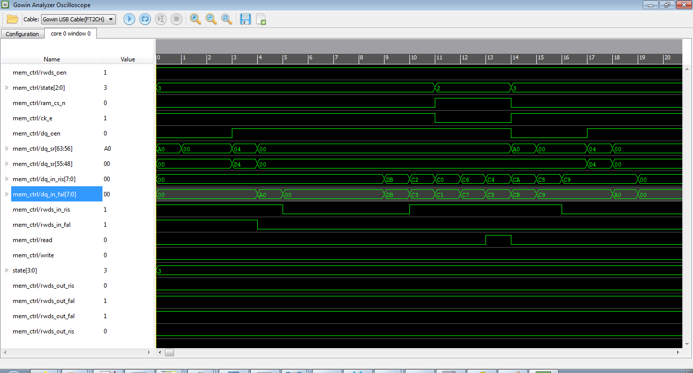
Can you explain why the memory keeps putting memory sample values on the bus after ck_e goes low. I'm talking about values on dq_in_ris and dq_in_fal after 10th clock cycle. 0xC3 and 0xC2 are proper values for adresses 0x0 and 0x1. But then goes 0xC1, 0xC0, 0xC7, 0xC6 which are correct values for next memory cells but shouldn't be here because ck_e is low.
I'm also having problems while trying to run the controller on clock frequencies of 30 MHz and below. Something is wrong with read waveforms and it reports "FAIL. Read wrong data."

The attached picture: blue trace: the "busy" output of the controller, the yellow trace the 'read' input signal.
The write operation does finish, but the read operation does not finish with the busy line constantly on. There is plenty of time for this to finish, the read is a 781kHz, which is 96 clock cycles and read should finish in at most 15.
After looking at the code, the width of the read clock should not matter, it might just do multiple reads, but the busy line should go down eventually.
Hi, just loaded up the library and test code. The test fails with "Read wrong data". Rather than use the Hashing of the address I also hard wired a value to write and then test read back but the result was the same. Not sure what's going on, I'm new to FPGA, but could some boards have a different SDRAM? With the GOWIN official example it works, although that only tests one byte at address 0.
I've tried to modify it to use O_psram_ck[1], IO_psram_rwds[1], O_psram_cs_n[1] and IO_psram_dq[15:8] to use the second W955D8MBYA psram die but I have not been able to get it to work.
Hi, I wondering it's possible to use this controller as VDP vram controller. I'm just porting an old project which uses a fast SRAM as VRAM but Tang Nano 9K doesn't have any SRAM onboard. Is this controller fast enough to provide 12MHz 16bit word reads?
Is there a way to change it in order to make a predictable access? I read it uses 12 clock latency for reads so 81MHz / 12 means = 6,775 M accesses/sec. I need to double it or at least let it grow up to 10.738635 MHz (my VDP clock). Any hint for me? Thanks.
A declarative, efficient, and flexible JavaScript library for building user interfaces.
🖖 Vue.js is a progressive, incrementally-adoptable JavaScript framework for building UI on the web.
TypeScript is a superset of JavaScript that compiles to clean JavaScript output.
An Open Source Machine Learning Framework for Everyone
The Web framework for perfectionists with deadlines.
A PHP framework for web artisans
Bring data to life with SVG, Canvas and HTML. 📊📈🎉
JavaScript (JS) is a lightweight interpreted programming language with first-class functions.
Some thing interesting about web. New door for the world.
A server is a program made to process requests and deliver data to clients.
Machine learning is a way of modeling and interpreting data that allows a piece of software to respond intelligently.
Some thing interesting about visualization, use data art
Some thing interesting about game, make everyone happy.
We are working to build community through open source technology. NB: members must have two-factor auth.
Open source projects and samples from Microsoft.
Google ❤️ Open Source for everyone.
Alibaba Open Source for everyone
Data-Driven Documents codes.
China tencent open source team.